Table of Contents
- 1.0 What is the AD8522AR? (The Precision Dual DAC)
- 1.1 Why Choose a Dual 12-Bit DAC?
- 1.2 Decoding the Part Number: AD8522AR
- 1.3 Key Features Overview
- 2.0 AD8522AR Pinout and Package Details
- 2.1 SOIC-14 Pin Configuration
- 2.2 Pin Functions: VDD, VREF, and SPI Lines
- 3.0 Programming the AD8522AR (SPI Interface)
- 3.1 The 3-Wire Serial Interface Explained
- 3.2 Sending Data: The 16-Bit Frame
- 4.0 Applications and Design Considerations
- 4.1 Where is the AD8522AR Used?
- 4.2 Design Tips: Reference Voltage Stability
In the realm of digital-to-analog conversion, engineers are often faced with a choice: sacrifice board space for multiple single-channel chips, or find a compact, integrated solution. For applications requiring precise voltage generation—such as servo control, programmable voltage sources, or calibration systems—the AD8522AR stands out as a classic, reliable choice.
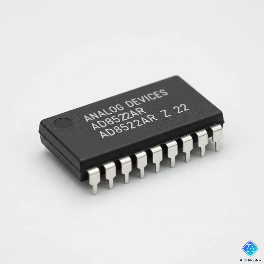
This component from Analog Devices is a Dual 12-Bit Voltage-Output DAC packaged in a space-saving SOIC-14. It combines high resolution (4096 steps) with the simplicity of a standard serial interface. Whether you are redesigning a legacy industrial controller or prototyping a new automated test rig, understanding the AD8522AR is key to achieving stable analog performance.
This guide provides a comprehensive technical overview of the AD8522AR, breaking down its datasheet, pinout, and programming requirements to help you integrate it seamlessly into your next design.
1.0 What is the AD8522AR? (The Precision Dual DAC)
The AD8522AR is a complete dual, 12-bit digital-to-analog converter. "Complete" in this context means it includes the necessary reference buffers and output amplifiers on-chip, simplifying the external circuit requirements.
1.1 Why Choose a Dual 12-Bit DAC?
A dual DAC is incredibly useful for systems that require coordinated analog outputs. * **Space Savings:** Replaces two separate DAC chips and their associated control wiring. * **Synchronization:** Both DACs can be updated simultaneously, which is critical for X-Y positioning systems or quadrature signal generation. * **12-Bit Precision:** Offers 4,096 discrete voltage steps. On a 0-4.096V scale, that's a precision of 1mV per step, ideal for fine control.1.2 Decoding the Part Number: AD8522AR
Let's break down the model number to ensure you have the right part: * **AD:** Manufacturer (Analog Devices). * **8522:** The specific device model (Dual 12-bit DAC). * **A:** Performance Grade. * **R:** Package Type. **"R"** signifies a **SOIC (Small Outline Integrated Circuit)** package, specifically the narrow 14-lead body.1.3 Key Features Overview
Here are the critical specifications from the **AD8522AR datasheet**:| Feature | Specification |
|---|---|
| Resolution | 12-Bits (Dual) |
| Supply Voltage | +5V Single Supply |
| Interface | 3-Wire Serial (SPI/QSPI/Microwire compatible) |
| Output Type | Voltage Output (Rail-to-Rail swing) |
| Settling Time | ~16 µs |
| Reference Input | External VREF (allows flexible output ranges) |
| Package | 14-Lead SOIC |
2.0 AD8522AR Pinout and Package Details
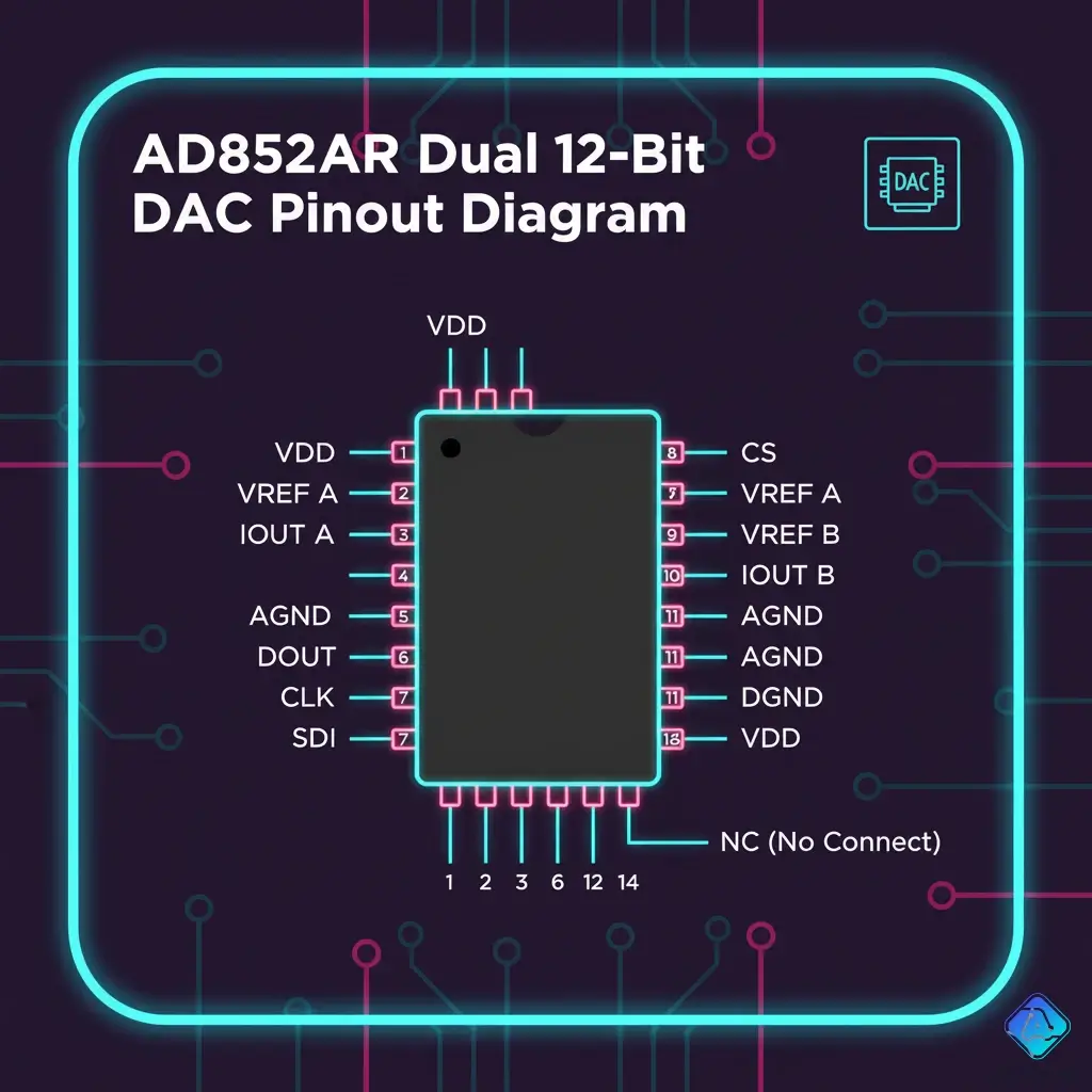
The AD8522AR comes in a standard 14-Lead SOIC package. This is a surface-mount package that is easy to handle for both prototyping and mass production.
2.1 SOIC-14 Pin Configuration

2.2 Pin Functions: VDD, VREF, and SPI Lines
* **Pin 1 (VDD):** Positive power supply, typically +5V. * **Pin 2 (GND):** Ground. * **Pin 3 (VREF A) & Pin 4 (VREF B):** Reference voltage inputs for DAC A and DAC B. These determine the full-scale output voltage range. * **Pin 5 (CS/LD):** Chip Select / Load DAC. Active low. This starts the data transfer and latches the data to the output. * **Pin 6 (CLK):** Serial Clock Input. Data is clocked in on the edge of this signal. * **Pin 7 (SDI):** Serial Data Input. * **Pin 13 (VOUT B) & Pin 14 (VOUT A):** The analog voltage output pins.3.0 Programming the AD8522AR (SPI Interface)
One of the AD8522AR's strengths is its simple 3-wire serial interface, which is compatible with standard SPI (Serial Peripheral Interface) ports found on microcontrollers like the Arduino, STM32, and PIC.
3.1 The 3-Wire Serial Interface Explained
The interface consists of **Clock (CLK)**, **Data (SDI)**, and **Chip Select (CS)**. 1. **Idle:** Set CS high. 2. **Start:** Pull CS low to initiate communication. 3. **Transfer:** Clock in the data bits on the SDI line. The device typically reads data on the rising or falling edge of the clock (check datasheet timing diagrams carefully). 4. **Latch:** Pull CS high again. This signals the end of the transmission and updates the DAC output voltage.3.2 Sending Data: The 16-Bit Frame
To control the DAC, you typically send a **16-bit data frame**: * **Address Bits:** The first few bits (usually 2 or more, depending on specific protocol nuances in the datasheet) select which DAC you are updating (DAC A, DAC B, or Both). * **Data Bits:** The following 12 bits represent the value you want to convert (0 to 4095). * **Padding/Control:** Any remaining bits.Example Logic (Conceptual):
[Address (2 bits)] [Data (12 bits)] [Dont Care (2 bits)]
(Note: Always verify the exact bit order—MSB vs. LSB first—in the official AD8522 datasheet).
4.0 Applications and Design Considerations
4.1 Where is the AD8522AR Used?
* **Digital Servo Control:** Controlling the position of motors and actuators with precision voltage signals. * **Programmable Power Supplies:** Setting the reference voltage for a larger voltage regulator. * **Digitally Controlled Calibration:** Replacing mechanical potentiometers (trimmers) with a DAC to allow software auto-calibration. * **Industrial Automation:** 4-20mA loop generation (when paired with a V-to-I converter).4.2 Design Tips: Reference Voltage Stability
The accuracy of the **AD8522AR** is only as good as the reference voltage (VREF) you provide. * **Do not use the 5V supply rail as VREF** if you need precision. The supply rail is often noisy. * **Use a dedicated Precision Voltage Reference IC** (like the ADR4525 or REF192) connected to Pins 3 and 4. * **Bypass Capacitors:** Always place a 0.1µF ceramic capacitor close to the VDD pin to filter out noise.In Conclusion
The AD8522AR Dual 12-Bit DAC is a testament to the "do one thing and do it well" philosophy. It provides two channels of high-precision analog output in a compact, easy-to-use package. Whether you are maintaining legacy industrial equipment or designing a new precision instrument, the AD8522AR offers the reliability and performance that Analog Devices is known for. By paying attention to your reference voltage and mastering the simple SPI interface, you can unlock the full potential of this versatile chip.
Ready to start your design? Browse our full selection of DACs to find the perfect component for your project.
Frequently Asked Questions
What is the difference between the AD8522AR and AD8522AN?
The primary difference is the package type. The **AD8522AR** uses a surface-mount **SOIC-14** package. The **AD8522AN** typically uses a through-hole **PDIP-14** package. Electrically, they are the same, but the "R" version is preferred for modern, compact PCB designs.
Can the AD8522AR output negative voltages?
No, the AD8522AR is a single-supply device. Its output swings from **0V to VREF** (or near VDD). To generate negative voltages, you would need an external op-amp circuit to shift and scale the output.
Is the AD8522AR compatible with Arduino?
Yes! You can easily drive the AD8522AR using an Arduino. Connect the DAC's SDI, CLK, and CS pins to the Arduino's SPI pins (MOSI, SCK, and a digital output for SS). You can use the standard `SPI.h` library to send the 16-bit command words.
What is the maximum VREF voltage?
The reference voltage input (VREF) generally should not exceed the supply voltage (VDD). If you are powering the chip with +5V, your VREF should be +5V or lower (e.g., 4.096V or 2.5V).
Where can I buy the AD8522AR?
The AD8522AR is a popular legacy component. You can find it at major distributors, or for hard-to-find stock and competitive pricing on ADI components, check out AichipLink's inventory.


