Table of Contents
- 1.0 What is the EP20K200EFC484-2? (Datasheet Explained)
- 1.1 The Altera APEX 20KE Family: A 1.8V Powerhouse
- 1.2 Decoding the Part Number: EP20K200EFC484-2
- 1.3 Obsolescence Status in 2025: A Critical Legacy Part
- 2.0 EP20K200EFC484-2 Key Technical Specifications
- 2.1 Core Logic, Memory, and I/O Specs
- 2.2 Operating Voltages and Package Details
- 2.3 EP20K200E vs. EP20K200: What's the Difference?
- 3.0 EP20K200EFC484-2 Pinout (FBGA-484 Package)
- 3.1 484-Ball FineLine BGA Pin Diagram
- 3.2 Key Pin Functions: Power, JTAG, and Configuration
- 4.0 Programming and Application Guide
- 4.1 Required Software: Legacy Altera Quartus II
- 4.2 Configuration and Booting
- 4.3 Common Legacy Applications
- 5.0 Frequently Asked Questions (FAQ)
If you're an engineer maintaining or repairing long-life-cycle equipment in the telecom, industrial, or defense sectors, the EP20K200EFC484-2 is a part number you'll recognize. This isn't a new chip, but it's a critical one. It hails from the Altera APEX 20KE family, a line of FPGAs that set the standard for density and on-chip memory in the early 2000s.
Why are we discussing a 20-year-old chip in 2025? Because the global market for Maintenance, Repair, and Operations (MRO) is a multi-billion dollar industry. A 2023 report on industrial automation highlighted that the average lifespan of factory equipment is now exceeding 15-20 years. When a control board on a $500,000 piece of machinery fails, you don't "just upgrade it." You repair it. And that repair often depends on sourcing one of these legacy FPGAs.
You're here for hard data, not a history lesson. This guide is your technical deep-dive into the EP20K200EFC484-2 datasheet. We'll cover its pinout, core specs, and the all-important (and tricky) legacy software required to work with it.
1.0 What is the EP20K200EFC484-2? (Datasheet Explained)
The EP20K200EFC484-2 is a high-density, 1.8V, SRAM-based Field-Programmable Gate Array (FPGA). It was manufactured by Altera (now Intel) and was a key member of the APEX 20KE family.
This family was significant because it was one of the first to be built on a 0.18-micron process, allowing for a massive increase in logic density and on-chip RAM compared to its predecessors. It was a true System-on-a-Chip (SoC) solution before the term was commonplace.
1.1 The Altera APEX 20KE Family: A 1.8V Powerhouse
The APEX 20KE family was designed for high-performance, logic-intensive, and data-centric applications. Its architecture was a major leap forward.
- MultiCore Architecture: It combined two key structures:
- Logic Array Blocks (LABs): The core of the FPGA, built from 10 Logic Elements (LEs) each, for implementing VHDL or Verilog.
- Embedded System Blocks (ESBs): These are large, flexible blocks of on-chip RAM. This was the key feature, allowing for deep FIFOs, processor cache, and buffers without using up general logic.
- 1.8V Core: This was a move from the older 5V and 3.3V devices, offering significant power savings.
- MultiVolt I/O: The I/O banks could be powered independently (e.g., at 3.3V, 2.5V) to interface with other chips without external level-shifters.
1.2 Decoding the Part Number: EP20K200EFC484-2
This specific part number is a detailed technical summary:
- EP20K: Identifies the device as a member of the APEX 20K family.
- 200E: The density of the device. This chip has 200,000 typical logic gates (8,320 LEs). The "E" signifies the enhanced 1.8V core.
- FC484: This is the package type: a 484-pin FineLine BGA (FBGA).
- -2: This is the speed grade. A
-2is a fast speed grade for this family.
1.3 Obsolescence Status in 2025: A Critical Legacy Part
Official Status: OBSOLETE / END-OF-LIFE (EOL)
Let's be perfectly clear: the EP20K200EFC484-2 and the entire APEX 20KE family are completely obsolete. They are no longer manufactured by Intel and are Not Recommended for New Designs (NRND).
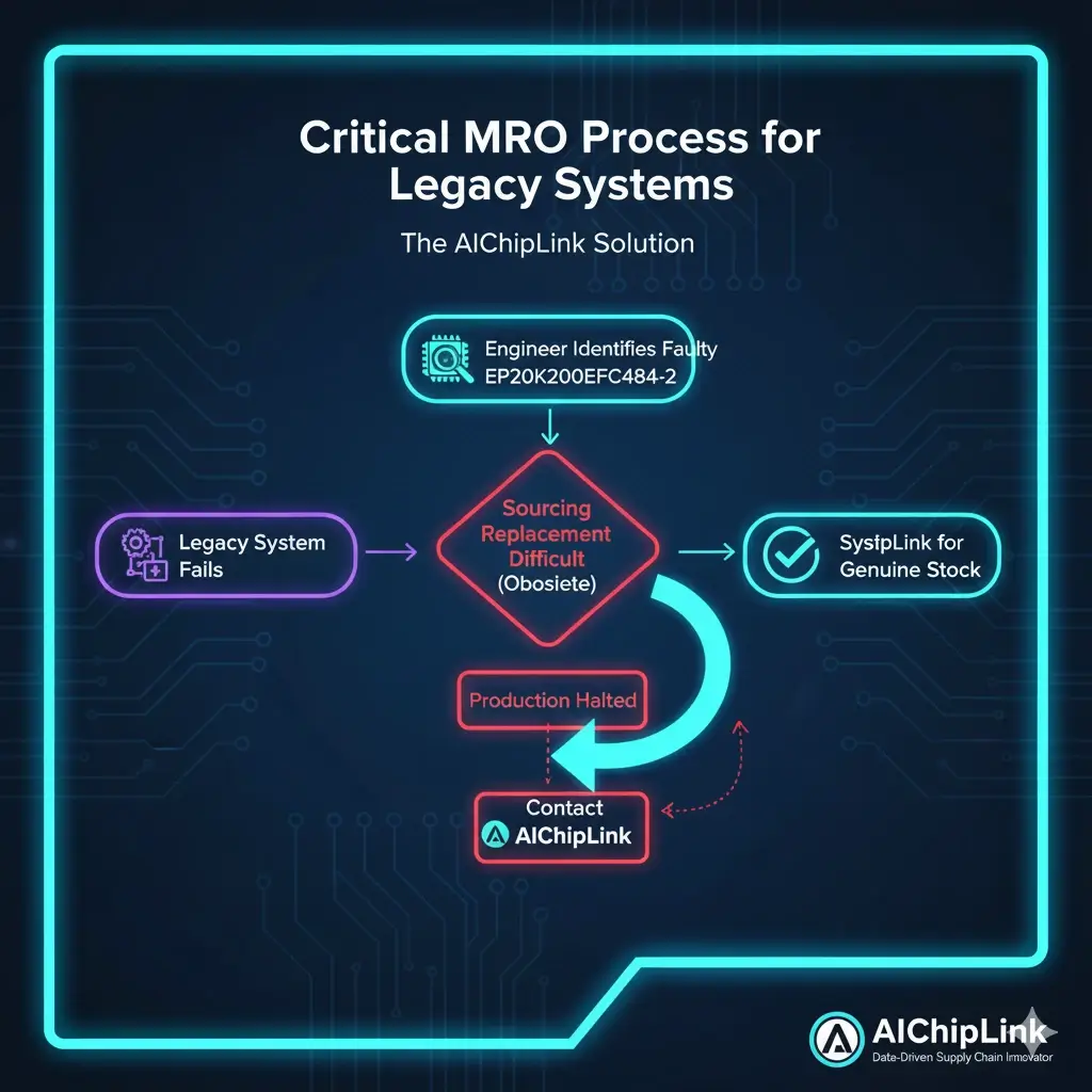
This part's entire value today is as a critical MRO (Maintenance, Repair, and Operations) component. Because it is in a specific 484-ball BGA package and has a unique architecture, there is no drop-in replacement. Repairing a board with a failed EP20K200EFC484-2 requires sourcing a genuine, identical part.
2.0 EP20K200EFC484-2 Key Technical Specifications
When you're sourcing a replacement, matching the EP20K200EFC484-2 specs is non-negotiable.
2.1 Core Logic, Memory, and I/O Specs
| Feature | Specification |
|---|---|
| Family | APEX 20KE |
| Logic Elements (LEs) | 8,320 |
| Logic Array Blocks (LABs) | 832 |
| Typical Logic Gates | 200,000 |
| Total RAM Bits | 106,496 (52 x ESBs of 2,048) |
| PLLs | 2 |
| Maximum User I/O | 376 |
| Package | 484-pin FineLine BGA |
2.2 Operating Voltages and Package Details
- Core Voltage (VCCINT): 1.8V
- I/O Voltage (VCCIO): 1.5V, 1.8V, 2.5V, or 3.3V (MultiVolt I/O)
- Temperature Range: Commercial (0°C to 85°C) or Industrial (-40°C to 100°C) - check your specific part marking.
- Package: 484-Ball FineLine BGA (23x23mm grid)
2.3 EP20K200E vs. EP20K200: What's the Difference?
This is a common point of confusion for buyers.
- EP20K200 (non-E): The original 2.5V core device.
- EP20K200E (the "E" model): The enhanced, lower-power 1.8V core device.
These two parts are NOT interchangeable. A board designed for the 1.8V "E" version will be damaged if a 2.5V part is installed, and a 1.8V part will not function in a 2.5V board.
3.0 EP20K200EFC484-2 Pinout (FBGA-484 Package)
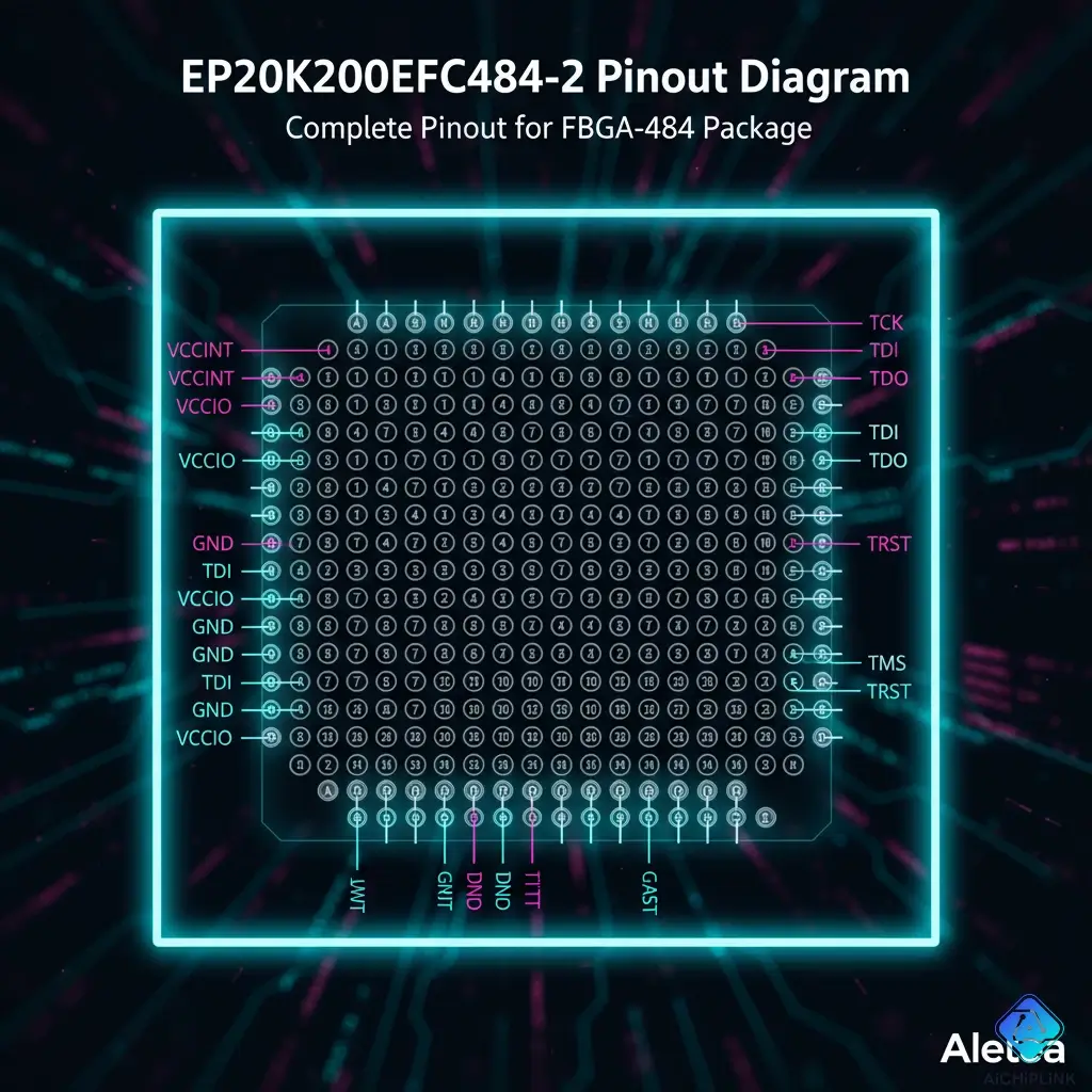
The EP20K200EFC484-2 pinout is a 484-ball FineLine BGA. This is a complex, high-pin-count package that requires a BGA rework station for replacement. You cannot troubleshoot this with a simple multimeter.
3.1 484-Ball FineLine BGA Pin Diagram

3.2 Key Pin Functions: Power, JTAG, and Configuration
When a board with this FPGA fails, engineers will check these critical support pins first.
- Power (VCCINT, VCCIO, VREFs): This chip has dozens of power and ground pins. VCCINT (1.8V) and VCCIO (e.g., 3.3V) must all be stable.
- Ground (GND): All ground balls must have a solid connection. A single cracked solder ball (a common BGA fault) can cause intermittent failures.
- JTAG Pins (TDI, TDO, TCK, TMS): The Joint Test Action Group port. This is the primary interface for programming, debugging, and testing the chip. If the JTAG chain is dead, the chip is unconfigurable.
- Configuration Pins (MSEL0, MSEL1): These pins are hard-wired on the PCB to set the configuration mode (e.g., Passive Serial, JTAG, etc.).
- Configuration Data (DATA, DCLK, nCONFIG, nSTATUS): These are the pins the FPGA uses to load its configuration from an external Altera EPC series configuration PROM.
4.0 Programming and Application Guide
4.1 Required Software: Legacy Altera Quartus II
This is the most critical hurdle for MRO. You cannot use modern Intel Quartus Prime software.
- Required Software: Altera Quartus II (legacy version).
- Compatible Version: Version 13.0sp1 is the last version of Quartus II that supports the APEX 20KE family.
- OS Compatibility: You will need to run this 32-bit software on an older OS, like Windows 7 or Windows XP (often in a virtual machine).
4.2 Configuration and Booting
The EP20K200EFC484-2 is SRAM-based, so its configuration is volatile (it's erased when power is lost).
- At Power-On: The FPGA wakes up blank.
- It must be configured by loading a bitstream file.
- This is usually done by an external, non-volatile Altera EPC series configuration PROM (e.g., an EPC2 or EPC16) that sits next to the FPGA on the board.
- The FPGA automatically reads from this PROM at boot-up. For testing, you can also load the configuration file directly via the JTAG port using a USB-Blaster cable.
4.0 Common Legacy Applications
You will find this FPGA in high-performance equipment from the early 2000s that is still in service.
- Telecommunications: The "E" series was ideal for 3G/4G base stations, network switches, and routers, where its large on-chip RAM was used for packet buffering.
- Industrial Control: High-speed machine vision systems, complex motor controllers, and large-scale PLC backplanes.
- Test & Measurement: The logic and RAM core for logic analyzers, protocol testers, and waveform generators.
- Aerospace & Defense: Long-life-cycle avionics and communications hardware.

Conclusion: A High-Performance Veteran
The EP20K200EFC484-2 was a titan of its time, enabling a wave of high-speed networking and data processing systems. Today, its role has shifted, but its importance has not diminished. For the thousands of critical systems still relying on this chip, it is an indispensable component.
Working with this FPGA requires specialized legacy knowledge, the right software, and a trusted supply chain. Sourcing a complex, high-pin-count BGA part that is long obsolete is a high-risk task. Don't let a counterfeit or improperly stored part take your system down.
If you are facing the challenge of sourcing this or other obsolete FPGAs, you need a partner who specializes in this market. Explore our full catalog of FPGAs or contact AichipLink today for a quote on the genuine, reliable legacy components you need.

Written by Jack Elliott from AIChipLink.
AIChipLink, one of the fastest-growing global independent electronic components distributors in the world, offers millions of products from thousands of manufacturers, and many of our in-stock parts is available to ship same day.
We mainly source and distribute integrated circuit (IC) products of brands such as Broadcom, Microchip, Texas Instruments, Infineon, NXP, Analog Devices, Qualcomm, Intel, etc., which are widely used in communication & network, telecom, industrial control, new energy and automotive electronics.
Empowered by AI, Linked to the Future. Get started on AIChipLink.com and submit your RFQ online today!
Frequently Asked Questions
What is the EP20K200EFC484-2?
The **EP20K200EFC484-2** is a legacy 1.8V core FPGA from the **Altera APEX 20KE** family. It features 8,320 Logic Elements (200,000 typical gates), over 100 kbits of on-chip RAM, and 376 user I/O pins. It comes in a 484-pin FineLine BGA package and has a fast "-2" speed grade.
Is the EP20K200EFC484-2 obsolete?
Yes, this part is **completely obsolete** and End-of-Life (EOL). It is no longer manufactured by Intel (Altera). Its only use today is as a replacement part for the **maintenance and repair (MRO)** of existing legacy systems.
What software is used to program the EP20K200EFC484-2?
You must use the legacy **Altera Quartus II** development software, specifically **version 13.0sp1 or older**. Modern Intel Quartus Prime software does **not** support the APEX 20KE family.
What is the difference between EP20K200E and EP20K200?
The **EP20K200E (the "E" version)** has a **1.8V** core. The older **EP20K200 (non-E)** has a **2.5V** core. They are **not** pin-compatible or interchangeable. Using the wrong one will damage the chip or the board.
What is a replacement for the EP20K200EFC484-2?
For repair, there is **no direct, pin-for-pin replacement**. You must source an identical **EP20K200EFC484-2**. For a new design, you would need to completely re-engineer the board to use a modern FPGA, which is a major project.


.png&w=256&q=75)


