Table of Contents
- 1.0 What is the LFEC3E-3Q208C? (Datasheet Explained)
- 1.1 The LatticeECP/EC Family: A Legacy 3.3V FPGA
- 1.2 Decoding the Part Number: LFEC3E-3Q208C
- 1.3 Obsolescence Status: A Critical MRO Part
- 2.0 LFEC3E-3Q208C Key Technical Specifications
- 2.1 Core Logic, Memory, and I/O Specs
- 2.2 Operating Voltages and Speed Grade
- 3.0 LFEC3E-3Q208C Pinout (QFP-208 Package)
- 3.1 208-Pin QFP Package Diagram
- 3.2 Key Pin Functions: Power, JTAG, Configuration
- 4.0 LFEC3E-3Q208C Programming, Applications, and Replacement
- 4.1 Required Software: Legacy Lattice ispLEVER
- 4.2 Configuration and Booting
- 4.3 Common Legacy Applications
- 4.4 Finding a Replacement
- 5.0 Frequently Asked Questions (FAQ)
1.0 What is the LFEC3E-3Q208C? (Datasheet Explained)
If you're an engineer, technician, or supply chain manager, you might encounter the LFEC3E-3Q208C FPGA when working on equipment that's been in the field for a decade or more. You won't find this chip in a new 2025-era design. This component is a veteran, a legacy workhorse from the LatticeECP / EC family, which was a go-to choice for low-cost, general-purpose FPGA applications in the 2000s.
Why are we talking about a 20-year-old chip? Because the global market for Maintenance, Repair, and Operations (MRO) for this legacy equipment is massive. A 2024 industry report on factory automation highlighted that the average lifespan of critical manufacturing equipment often exceeds 15-20 years. When a control board on a $100,000 piece of test equipment or a factory PLC line fails, you don't "just upgrade it." You repair it.
And that repair often hinges on sourcing this one specific, obsolete component. This guide is your technical deep-dive into the LFEC3E-3Q208C datasheet. We'll cover its specs, pinout, and the critical (and tricky) legacy software you need to work with it.
1.1 The LatticeECP/EC Family: A Legacy 3.3V FPGA
The LatticeECP/EC family (Economy Plus / Economy) was designed to hit a sweet spot: provide more logic density and features than a CPLD, but at a much lower cost than high-performance FPGAs. It was built on a 1.8V core with 3.3V I/O, making it a bridge between older 5V systems and modern low-voltage logic.
Its core value proposition was:
- Low Cost: Purpose-built to be an economical FPGA solution.
- SRAM-Based: Like all modern FPGAs, its configuration is volatile and must be loaded from an external flash chip at power-on.
- Rich Feature Set: It was one of the first low-cost families to include dedicated Embedded Block RAM (EBR) and Phase-Locked Loops (PLLs) for clock management.
1.2 Decoding the Part Number: LFEC3E-3Q208C
The part number is a technical code that tells you exactly what you're holding.
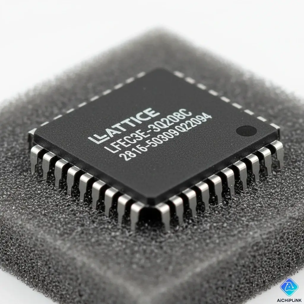
- LFEC: This identifies the device as a LatticeECP (Economy Plus) family FPGA.
- 3: The device density. This chip has 3,000 Logic Cells (LCs).
- E: This is an additional identifier for the ECP "E" family.
- -3: This is the speed grade. For Lattice, a lower number is faster. A
-3is the fastest speed grade available for this device. - Q208: This is the package. Q = Quad Flat Pack (QFP). 208 = 208 pins.
- C: This is the temperature grade. C = Commercial, with an operating range of 0°C to 85°C.
1.3 Obsolescence Status: A Critical MRO Part
Official Status: OBSOLETE / END-OF-LIFE (EOL)
Let's be clear: the LFEC3E-3Q208C and the entire LatticeECP/EC family are completely obsolete. They are no longer manufactured by Lattice and are Not Recommended for New Designs (NRND).
This part's entire value today is as a critical MRO (Maintenance, Repair, and Operations) component. Because of its specific pinout, 3.3V I/O, and legacy software requirements, there is no modern, drop-in replacement. Repairing a board with a failed LFEC3E requires sourcing a genuine, identical part.
2.0 LFEC3E-3Q208C Key Technical Specifications
When you're sourcing a replacement, matching the LFEC3E-3Q208C specs is non-negotiable.
2.1 Core Logic, Memory, and I/O Specs
This table summarizes the core resources available on this device.
| Feature | Specification |
|---|---|
| Family | LatticeECP / EC |
| Logic Cells (LCs) | 3,000 |
| Total RAM Bits | 57,344 bits (12 x 4.5-kbit EBRs) |
| Embedded Block RAM (EBRs) | 12 |
| PLLs | 2 |
| Maximum User I/O | 147 |
| Technology | SRAM-based CMOS |
| Package | 208-Pin QFP |

2.2 Operating Voltages and Speed Grade
This is a critical specification for any MRO work.
- Core Voltage (VCC): 1.8V (± 5%)
- I/O Voltage (VCCIO): 3.3V (Also supports 2.5V, 1.8V, 1.5V)
- Package: 208-Pin Plastic Quad Flat Pack (PQFP)
- Temperature Range: Commercial (0°C to 85°C)
- Speed Grade: -3 (This is the fastest grade. A
-3part can replace a slower-4or-5part, but you cannot use a-4to replace a-3.)
3.0 LFEC3E-3Q208C Pinout (QFP-208 Package)
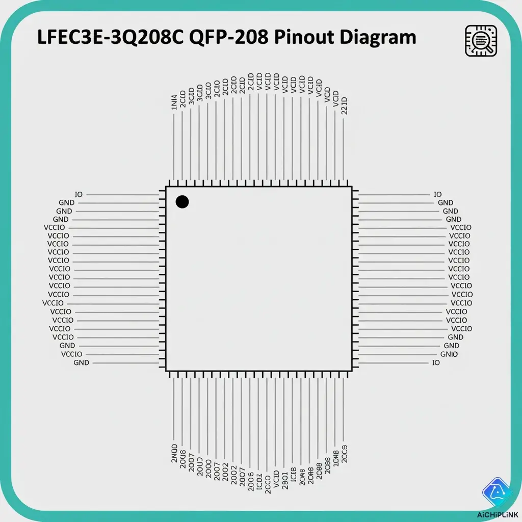
If you're troubleshooting a dead board, the LFEC3E-3Q208C pinout is your map. The QFP-208 is a 208-pin surface-mount package with 52 "gull-wing" leads on each of its four sides.
3.1 208-Pin QFP Package Diagram

3.2 Key Pin Functions: Power, JTAG, Configuration
When a board fails, you don't probe all 147 I/O pins. You check the "housekeeping" pins first.
| Pin Type | Name(s) | Function |
|---|---|---|
| Core Power | VCC | 1.8V core logic supply. There are multiple of these pins. |
| I/O Power | VCCIO (Banks 0-7) | 3.3V (or 2.5V, etc.). Each I/O bank has its own power. |
| Ground | GND | Numerous ground pins. All must be connected. |
| JTAG | TDI, TDO, TCK, TMS | The 4-pin JTAG port. Used for programming, debugging, and testing. |
| Config Mode | MSEL[2:0] | These pins are hard-wired on the PCB (high or low) to set the configuration mode (e.g., Master SPI, Slave Serial, etc.). |
| Config Data | CCLK, CDONE, PROGRAMN | The pins that control and monitor the configuration process. If CDONE (Config Done) is low, the FPGA is not booted. |
4.0 LFEC3E-3Q208C Programming, Applications, and Replacement
This is the most critical information for an engineer in 2025. How do you program this chip, and what do you do if you can't find one?
4.1 Required Software: Legacy Lattice ispLEVER
This is the single biggest hurdle for working with these parts. You cannot use modern Lattice Radiant or Lattice Diamond software.
- Required Software: You must find and install the original Lattice ispLEVER Classic software.
- Compatible Version: ispLEVER Classic 1.4 is a version known to support the LatticeECP/EC family.
- OS Compatibility: This legacy software is 32-bit and was designed for Windows XP. You will need to run this on a dedicated older machine or in a virtual machine (VM) to use it.
- Programming Hardware: You need a compatible JTAG programming cable, such as the Lattice ispDOWNLOAD cable (e.g., HW-USB-1B).
4.2 Configuration and Booting
The LFEC3E-3Q208C is SRAM-based, so its configuration is volatile (it's erased when power is lost). It must be programmed every time it's powered on.
- At Power-On: The FPGA wakes up blank.
- It needs to be configured by loading a bitstream file.
- This is usually done by an external, non-volatile Lattice, Altera, or Xilinx serial PROM (e.g., a Lattice ispPAC-POWR chip or a standard SPI flash) that sits next to the FPGA on the board.
- The FPGA automatically reads from this PROM at boot-up (Master SPI mode) or can be configured by a host processor (Slave Serial/Parallel modes).
4.3 Common Legacy Applications
You will find the LFEC3E-3Q208C in long-life industrial, medical, and telecom equipment built in the 2000s.
- Industrial Control: As the logic core for PLCs, motor controllers, and robotics.
- Telecommunications: In legacy switching hardware and line cards.
- Test & Measurement: The logic core for older oscilloscopes, spectrum analyzers, and waveform generators.
- "Glue Logic": Its most common use. It replaces dozens of smaller logic chips, connecting a CPU to its memory, peripherals, and I/O.
4.4 Finding a Replacement
You have one main challenge: this part is obsolete.
- Direct Replacement: The only 100% drop-in, pin-compatible replacement is another LFEC3E-3Q208C. As this is the fastest speed grade, it can replace a slower
-4or-5part. - Modern Redesign: There is no modern, pin-compatible replacement. A redesign would mean using a modern, low-voltage FPGA (like a Lattice iCE40 or MachXO) and then redesigning the entire PCB to accommodate the new footprint and voltage levels. This is a massive, expensive engineering project.
| Parameter | LFEC3E-3Q208C (Legacy) | Modern FPGA (e.g., Lattice iCE40) |
|---|---|---|
| Core Voltage | 1.8V | ~1.2V |
| Logic Cells | 3,000 | 5,000+ |
| Package | 208-pin QFP | 100-pin BGA (or smaller) |
| Software | ispLEVER Classic (Legacy) | Lattice Radiant (Modern) |
| Status | Obsolete | In Production |
[Insert infographic: A simple flowchart showing the MRO process: 1. System Fails -> 2. Engineer identifies faulty LFEC3E-3Q208C -> 3. Sourcing is difficult (Obsolete) -> 4. Contact AichipLink for genuine legacy parts -> 5. System Repaired.] Alt Text: A flowchart showing the MRO process for a legacy FPGA like the LFEC3E-3Q208C.
Conclusion: The MRO Challenge of a 3.3V Workhorse
The LFEC3E-3Q208C FPGA is a true classic. It represents a generation of FPGAs that brought the power of on-chip RAM and PLLs to the low-cost, general-purpose market. Today, its role has shifted from innovation to sustainment. For the thousands of critical systems worldwide built around this chip, it remains an indispensable component.
Working with this device requires specialized legacy knowledge, the right (and very old) software, and a trusted supply chain. Sourcing a 20-year-old part is a high-risk task. You cannot afford to risk a line-down situation on a counterfeit or improperly stored component.
If you are facing the challenge of sourcing this or other "unobtanium" legacy FPGAs, you need a partner who understands the MRO market.
Explore our full catalog of FPGAs contact AichipLink today. We are experts in sourcing hard-to-find and obsolete components, and we can help you get the genuine parts you need to keep your legacy systems operational.

Written by Jack Elliott from AIChipLink.
AIChipLink, one of the fastest-growing global independent electronic components distributors in the world, offers millions of products from thousands of manufacturers, and many of our in-stock parts is available to ship same day.
We mainly source and distribute integrated circuit (IC) products of brands such as Broadcom, Microchip, Texas Instruments, Infineon, NXP, Analog Devices, Qualcomm, Intel, etc., which are widely used in communication & network, telecom, industrial control, new energy and automotive electronics.
Empowered by AI, Linked to the Future. Get started on AIChipLink.com and submit your RFQ online today!
Frequently Asked Questions
What is the LFEC3E-3Q208C?
The **LFEC3E-3Q208C** is a legacy 1.8V core, 3.3V I/O, SRAM-based **FPGA** from the LatticeECP (Economy Plus) family. It features 3,000 Logic Cells, 57 kbits of RAM, and 147 user I/O pins. It is in a 208-pin Plastic Quad Flat Pack (QFP) and is rated for the commercial temperature range with a -3 (fast) speed grade.
Is the LFEC3E-3Q208C obsolete?
Yes, this part is **completely obsolete** and End-of-Life (EOL). It is no longer manufactured by Lattice and is not recommended for new designs. Its only use today is as a replacement part for maintenance and repair (MRO) of very old equipment.
What software do I use to program the LFEC3E-3Q208C?
You must use the legacy **Lattice ispLEVER Classic** software. The modern Lattice Radiant and Lattice Diamond software suites **do not** support the LatticeECP/EC family. You will likely need a 32-bit OS (like Windows XP/7) to run this old software.
What is the difference between LFEC3E-3Q208C and LFEC3E-5Q208C?
The only difference is the **speed grade**. The **-3** part is the **fastest** speed grade. The **-5** part is the **slowest**. A `-3` part can always be used as a direct replacement for a `-5` part, but you cannot replace a `-3` with a `-5` as it may violate the system's timing requirements.
What is a replacement for the LFEC3E-3Q208C?
There is **no direct, pin-for-pin modern replacement**. For a repair, you must source an identical **LFEC3E-3Q208C**. A full system redesign is the only other (and very costly) alternative.