Table of Contents
- 1.0 What is the MPC8264AZUPIBB? (Datasheet Explained)
- 1.1 The PowerQUICC II Family: A Legacy Powerhouse
- 1.2 The Dual-Core Architecture: PowerPC Core + CPM
- 1.3 Decoding the Part Number: MPC8264AZUPIBB
- 2.0 MPC8264AZUPIBB Key Technical Specifications
- 2.1 Core Processor and Bus Specs
- 2.2 Communications Processor Module (CPM) Features
- 2.3 Operating Conditions and Power
- 3.0 MPC8264AZUPIBB Pinout (TBGA-516 Package)
- 3.1 516-Ball TBGA Package Details
- 3.2 Key Pin Functions (Power, JTAG, Network I/O)
- 4.0 MPC8264AZUPIBB Applications & Legacy Status
- 4.1 Common Legacy Applications (Routers, Switches)
- 4.2 How to Program the MPC8264 (Software & Tools)
- 4.3 Obsolescence & Replacement in 2025
- 5.0 Frequently Asked Questions (FAQ)
If you're an engineer maintaining a piece of networking or telecommunications equipment from the early 2000s, you've likely come across this chip. The MPC8264AZUPIBB is not a simple microcontroller; it's a high-performance, 32-bit communications processor that was the engine for a generation of routers, switches, and 3G base stations. Its failure can bring down a critical piece of infrastructure, and you've just been tasked with fixing it.
You're in a tough spot. This chip is a complex, legacy component. You can't just swap it for a modern equivalent. The global market for MRO (Maintenance, Repair, and Operations) for legacy telecom and industrial hardware is valued in the billions, precisely because components like the MPC8264AZUPIBB are so specialized and difficult to source.
You don't need a sales pitch; you need a technical deep dive. This guide is your engineering-focused breakdown of the MPC8264AZUPIBB datasheet, explaining its unique architecture, pinout, and what you need to know to manage it in 2025.
1.0 What is the MPC8264AZUPIBB? (Datasheet Explained)
The MPC8264AZUPIBB is a member of the PowerQUICC II family of integrated communications processors, originally developed by Motorola, then Freescale, and now owned by NXP Semiconductors. It was designed specifically for high-bandwidth networking applications.
1.1 The PowerQUICC II Family: A Legacy Powerhouse
The PowerQUICC II family was the industry standard for networking equipment for nearly a decade. Its primary function was to combine a powerful general-purpose processor with a dedicated networking co-processor, all on a single chip. This allowed equipment to handle high-speed data packets (like Ethernet or ATM) without overburdening the main CPU.
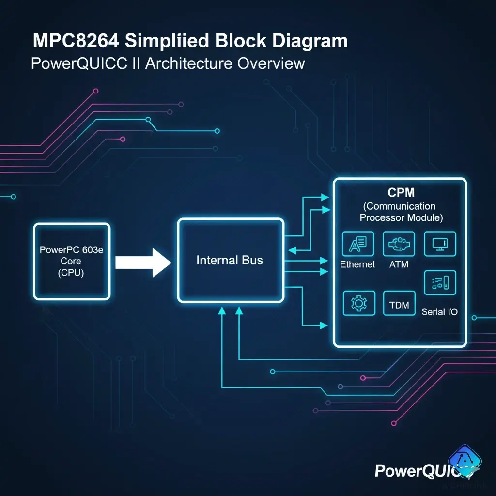
1.2 The Dual-Core Architecture: PowerPC Core + CPM
This is the most critical concept to understand about the MPC8264: it is a dual-core processor, but not in the modern sense.
- Host Processor (CPU): It has a high-performance PowerPC 603e core (G2 core). This is the "brain" that runs the operating system (like Linux or VxWorks), the routing tables, and the management software.
- Co-Processor (CPM): It has a separate 32-bit RISC Communications Processor Module (CPM). This is the "brainstem" that handles all the real-time, high-speed networking tasks. It manages the Ethernet MACs, ATM segmentation, and other I/O, allowing the main CPU to focus on high-level tasks.
Analogy: Think of the PowerPC core as the CEO of a company, making strategic decisions. The CPM is the entire shipping and logistics department, handling all the incoming and outgoing packages at high speed so the CEO doesn't have to.

1.3 Decoding the Part Number: MPC8264AZUPIBB
The part number is a technical resume:
- MPC8264A: The specific device model with revision 'A'.
- ZU: The package type, a 516-pin TBGA (Tape Ball Grid Array).
- P: The processor core frequency, which is 266 MHz.
- I: The temperature grade, Industrial (-40°C to 85°C).
- BB: A feature or revision code.
2.0 MPC8264AZUPIBB Key Technical Specifications
When you're sourcing a replacement, matching the MPC8264AZUPIBB specs is vital.
2.1 Core Processor and Bus Specs
| Feature | Specification |
|---|---|
| Host Processor Core | PowerPC 603e (G2 Core) |
| Host Processor Speed | 266 MHz |
| Bus Frequency | 133 MHz (max) |
| L1 Cache | 16 KB (Instruction) / 16 KB (Data) |
| System Bus | 60x Bus (64-bit data, 32-bit address) |
| Memory Controller | Supports SDRAM, SRAM, EPROM |
2.2 Communications Processor Module (CPM) Features
This is what makes the chip a communications processor. The CPM has its own 32-bit RISC core and controls a host of network interfaces:
- Fast Ethernet: Up to three 10/100 Mbps Ethernet controllers (FECs).
- ATM: An ATM (Asynchronous Transfer Mode) controller for telecom backbone interfacing.
- TDM/Serial: Multiple serial controllers (SCCs, SMCs) for T1/E1, HDLC, and other WAN protocols.
- I²C and SPI: For interfacing with local peripherals like sensors or boot PROMs.
2.3 Operating Conditions and Power
| Feature | Specification |
|---|---|
| Core Voltage (VDD) | 1.8V |
| I/O Voltage (VDDQ) | 3.3V |
| Package | 516-pin TBGA (Tape Ball Grid Array) |
| Temperature Range | Industrial (-40°C to 85°C) |
3.0 MPC8264AZUPIBB Pinout (TBGA-516 Package)
The MPC8264AZUPIBB pinout is a complex, 516-ball grid array. This is not a hobbyist-friendly package; it requires precise, automated SMT placement and X-ray inspection.
3.1 516-Ball TBGA Package Details
When you're inspecting a board, you won't see pins, but a grid of solder balls on the underside of the chip. A failure here is often due to a cracked or cold solder joint, which can only be fixed with a BGA rework station.
3.2 Key Pin Functions (Power, JTAG, Network I/O)
You can't probe all 516 pins, but here are the key groups to be aware of:
- Power: Dozens of pins for the 1.8V core (VDD) and 3.3V I/O (VDDQ) supplies, plus their associated grounds.
- System Bus: The 64-bit data bus and 32-bit address bus pins that connect to the main system SDRAM and Flash memory.
- CPM Network I/O: These are the physical I/O pins for the Ethernet (MII/RMII), ATM, and TDM ports.
- JTAG/COP: These are the most critical pins for debugging. The JTAG/COP port is the only way for a developer to halt the processor, load code, and debug a non-functional board.
4.0 MPC8264AZUPIBB Applications & Legacy Status
This chip was a high-performance part for its time, and you'll find it in equipment that was the backbone of the internet.
4.1 Common Legacy Applications (Routers, Switches)
* **Enterprise Routers and Switches** * **DSLAMs (Digital Subscriber Line Access Multiplexers)** * **3G Wireless Base Stations** * **VoIP (Voice over IP) Media Gateways** * **Industrial Control Systems**4.2 How to Program the MPC8264 (Software & Tools)
You cannot program this chip with an Arduino IDE. It requires a professional (and often legacy) development environment.
- Board Support Package (BSP): You need a BSP for the specific board, typically for an RTOS like VxWorks, Green Hills Integrity, or a legacy embedded Linux (e.g., 2.4 or 2.6 kernel).
- Toolchain: A PowerPC cross-compiler is required (e.g., GCC for PowerPC, or a proprietary IDE like Wind River Workbench or Green Hills MULTI).
- Debugger: To load code and debug a board, you must use a JTAG or BDI (Background Debug Interface) probe, such as a BDI2000/3000.
- CPM Microcode: The Communications Processor Module (CPM) itself must be initialized with its own microcode to configure the network interfaces before the main CPU can use them.
This process is complex and highly specialized, which is why repairing these systems is a non-trivial task. This video, while for a different PowerQUICC, gives you an idea of the legacy CodeWarrior development environment used for these chips.
4.3 Obsolescence & Replacement in 2025
Official Status: Obsolete / End-of-Life (EOL)
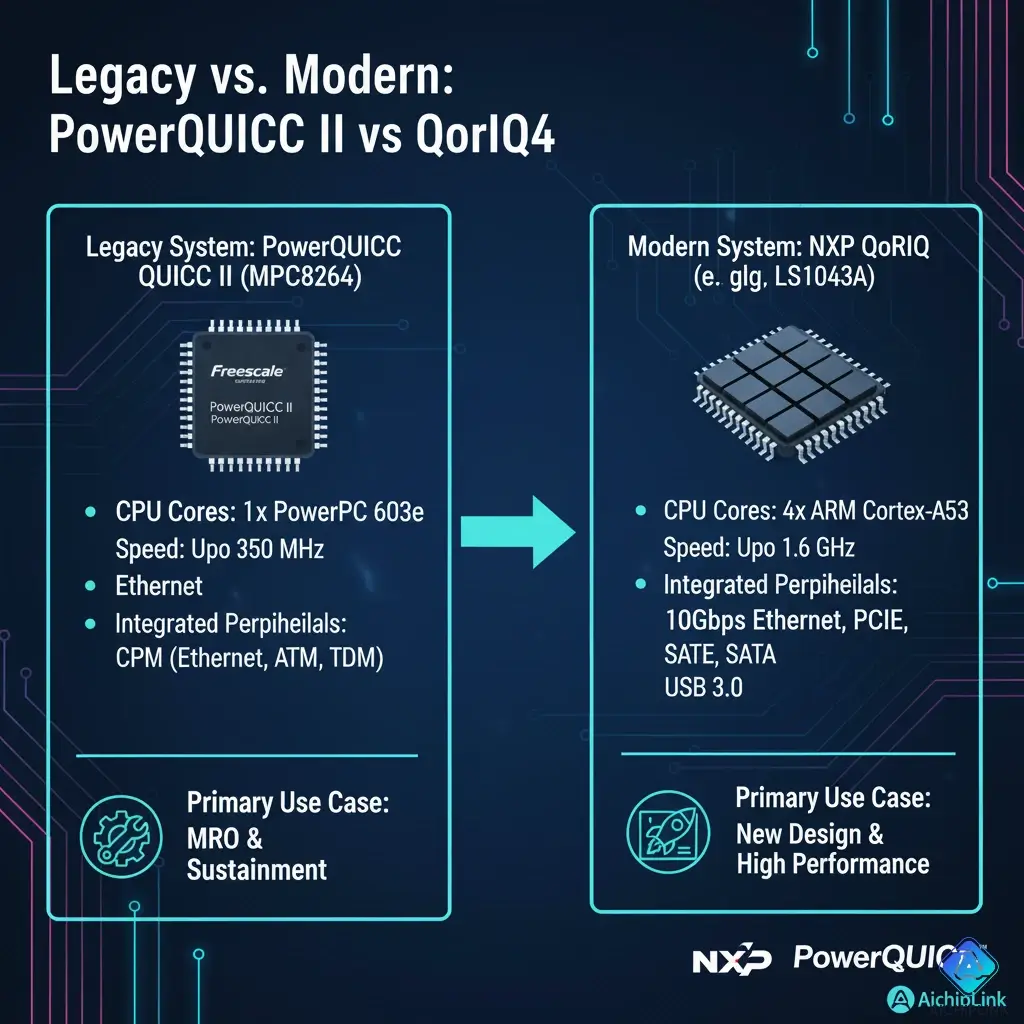
The MPC8264AZUPIBB is a legacy component. It is Not Recommended for New Designs (NRND). The entire PowerQUICC II family has been superseded by newer platforms (like NXP's QorIQ series).
This means there is no modern, pin-compatible replacement. If your system has a failed MPC8264, the only solution for repair is to source a genuine, identical MPC8264AZUPIBB. This makes a reliable supply chain for legacy parts absolutely critical.

Conclusion: A Specialized Core for Legacy Infrastructure
The MPC8264AZUPIBB is not just another part number; it's a highly integrated system-on-a-chip that was the engine for a generation of networking hardware. Its complex dual-core architecture (PowerPC + CPM) made it powerful, but today, it makes it a significant MRO challenge.
As an engineer or supply chain manager, you know that a "line-down" situation costs more than just the price of a chip. It costs time, labor, and customer trust. Don't let a hard-to-find part be your bottleneck.
AichipLink specializes in sourcing high-quality, genuine legacy components, including communications processors from the PowerQUICC family. If you need to secure your supply of the MPC8264AZUPIBB, contact us today for a quote and keep your critical infrastructure running.

Written by Jack Elliott from AIChipLink.
AIChipLink, one of the fastest-growing global independent electronic components distributors in the world, offers millions of products from thousands of manufacturers, and many of our in-stock parts is available to ship same day.
We mainly source and distribute integrated circuit (IC) products of brands such as Broadcom, Microchip, Texas Instruments, Infineon, NXP, Analog Devices, Qualcomm, Intel, etc., which are widely used in communication & network, telecom, industrial control, new energy and automotive electronics.
Empowered by AI, Linked to the Future. Get started on AIChipLink.com and submit your RFQ online today!
Frequently Asked Questions
What is the MPC8264AZUPIBB?
The MPC8264AZUPIBB is a high-performance, 32-bit communications processor from the Freescale (Motorola) PowerQUICC II family. It features a PowerPC 603e core (266 MHz) and a separate Communications Processor Module (CPM) RISC core for handling network protocols. This specific part has an industrial temperature rating and comes in a 516-pin TBGA package.
Is the MPC8264AZUPIBB obsolete?
Yes, the MPC8264AZUPIBB is a mature, legacy component. It is End-of-Life (EOL) and Not Recommended for New Designs (NRND). It is primarily sourced today for the maintenance, repair, and operation (MRO) of long-lifecycle industrial, networking, and telecommunications equipment.
What is the difference between the PowerPC core and the CPM in the MPC8264?
The MPC8264 is a dual-core processor. The main PowerPC 603e core (the 'host processor') runs the main operating system and application (e.g., routing tables, management). The Communications Processor Module (CPM) is a separate 32-bit RISC co-processor that offloads the low-level, real-time networking tasks (like managing Ethernet MACs, ATM, or TDM) from the main CPU.
What software do I use to program an MPC8264?
You need a specialized legacy toolchain. This typically includes a PowerPC C/C++ cross-compiler (like GCC or the one in CodeWarrior) and a Board Support Package (BSP) for a real-time operating system like VxWorks or a legacy embedded Linux kernel. You also need a JTAG or BDI debug probe to load the software onto the hardware.
What is a replacement for the MPC8264AZUPIBB?
For repair, there is no direct, pin-compatible replacement. You must source an identical MPC8264AZUPIBB. For a new design, you would migrate to a modern multi-core processor from NXP's QorIQ family or another ARM-based networking SoC, which would require a complete hardware and software redesign.